 Power Conversion Engineering
Talk to an engineer (888) 597-9255
Products Power Conversion Engineering Explore our engineering-grade switching power adapters, wall-mount chargers, linear transformers, and industrial power supplies designed for global regulatory compliance.
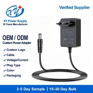
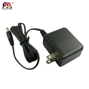
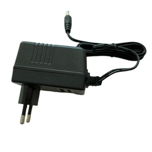

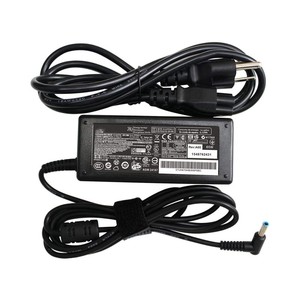
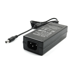
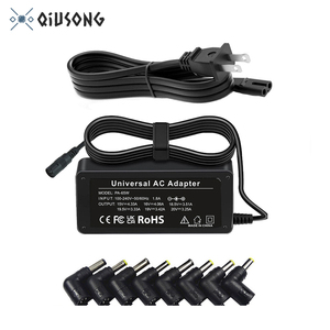
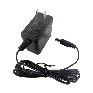
A comprehensive technical analysis of circuit topology selection, thermal management protocols, EMI mitigation strategies, and high-density power conversion paradigms in modern manufacturing.
In the highly competitive landscape of industrial electronics, medical devices, and telecommunications equipment, the election of the fundamental power conversion topology establishes the ceiling for electrical efficiency, physical power density, electromagnetic compatibility (EMC), and overall system reliability. As a primary China switching power manufacturer, our engineering framework integrates modern power topologies tailored directly to input voltage profiles, power output demands, and severe ambient stress factors.
For low to mid-power applications spanning 1 Watt to 75 Watts (such as wall-mount external AC adapters, embedded IoT power node regulators, and compact auxiliary rails), the Quasi-Resonant (QR) Flyback Topology remains the operational gold standard. By modulating the switching frequency so that the primary MOSFET turns on at the minimum valley of the drain-to-source voltage waveform, QR flyback significantly reduces capacitive turn-on losses compared to traditional continuous conduction mode (CCM) topologies. When paired with secondary Synchronous Rectification (SR) ICs, efficiency ratings comfortably cross the 90% threshold, facilitating compliance with DoE Level VI and EU CoC Tier 2 stringent standby and active efficiency metrics.
When operational parameters demand output levels between 100 Watts and 3,600 Watts—typical of medical diagnostic carts, high-density industrial control cabinets, and electric vehicle charging infrastructure—the architecture shifts toward LLC Resonant Half-Bridge Converters integrated with interleaved Active Power Factor Correction (PFC) front-ends. The LLC resonant topology leverages soft-switching Zero Voltage Switching (ZVS) across the primary switches and Zero Current Switching (ZCS) across the secondary rectifier diodes over the entire load spectrum. This completely eliminates hard switching spikes, exponentially reduces electromagnetic interference (EMI) at the source, and elevates efficiency levels up to 96.5%.
The practical physical limits of legacy Silicon (Si) MOSFETs have triggered an industry-wide transition toward Wide Bandgap (WBG) materials, specifically Gallium Nitride (GaN) and Silicon Carbide (SiC). GaN high-electron-mobility transistors (HEMTs) exhibit critical field breakdown parameters nearly ten times higher than silicon, alongside electron mobility rates that allow switching frequencies to scale from standard 65kHz-100kHz bands up into the multi-megahertz regime.
By engineering our latest OEM/ODM switching power supplies with GaN-on-Si integrated power stages, internal magnetic components (transformers and common-mode chokes) undergo a dramatic reduction in physical volume—frequently exceeding 40% to 50% spatial reduction compared to legacy silicon designs. Furthermore, the absence of reverse recovery charge ($Q_{rr}$) in GaN devices drastically simplifies EMI filter design, eliminating bulky passive components and lowering high-frequency radiated emissions.
For high-power, high-voltage industrial applications (input DC buses spanning 310V to 800V DC), Silicon Carbide (SiC) Schottky Barrier Diodes and SiC MOSFETs serve as the structural backbone. SiC exhibits superior thermal conductivity (3.7 W/cm·K versus 1.3 W/cm·K for Si), allowing power supplies to operate reliably at junction temperatures exceeding +175°C without experiencing thermal runaway. This capability is critical for fanless, conduction-cooled power enclosures deployed in sealed industrial automation cells and harsh military environments.
Utilizing high thermal conductivity potting compounds (silicone/epoxy resins up to 1.5 W/m·K), aluminum baseplates, and finite element thermal modeling to eliminate hot-spots, ensuring operational reliability from -40°C up to +85°C ambient without forced-air cooling.
Multistage differential and common-mode line filters combined with primary-to-secondary Y1/Y2 safety capacitors allow all designs to surpass CISPR 32 / EN 55032 Class B radiated and conducted emissions requirements with >6dB margin.
Reinforced double-insulation schemes providing 3,000VAC to 4,000VAC isolation voltage. Transformer construction incorporates triple-insulated wire (TIW) and margin tape to satisfy strict creepage and clearance distances mandated by IEC 60601-1 (2xMOPP).
Compare performance metrics, switching characteristics, safety isolation standards, and targeted industrial applications across primary power conversion platforms.
| Topology Platform | Power Range | Efficiency Benchmark | Isolation Rating | EMC Compliance | Target Application Spectrum |
|---|---|---|---|---|---|
| Flyback (Quasi-Resonant) | 1W – 75W | 85% – 91% | 3,000VAC / 4,242VDC | EN55032 Class B | Wall Adapters, IoT Endpoints, Router Power, Smart Home Devices |
| Active Clamp Flyback (GaN) | 45W – 140W | 92% – 94.5% | 3,750VAC Reinforced | CISPR 32 Class B | Ultra-Compact Mobile Chargers, Medical Monitors, Portable Testing |
| Single-Ended Forward | 75W – 200W | 88% – 92% | 3,000VAC Standard | EN55022 / FCC Part 15 | Telecom DC-DC Converters, Industrial Controllers, Motor Drives |
| LLC Resonant + PFC | 150W – 1,200W | 93% – 96.5% | 4,000VAC (2xMOPP) | EN61000-3-2 Class D | Medical Diagnostic Equipment, Server Racks, High-Bay LED Systems |
| Phase-Shifted Full-Bridge | 1,000W – 3,600W+ | 94% – 97% | 2,500VAC to 4,000VAC | MIL-STD-461G / EN55011 | EV Charging Stations, Heavy Automation, Defense Ground Power |
Strategic analysis for global procurement teams, sourcing executives, and system architects navigating the evolving power supply supply chain.
Traditional analog feedback loops utilizing optocouplers and TL431 shunt regulators are rapidly giving way to Digital Signal Processors (DSP) and microcontroller-driven control loops. Digital power management enables real-time parameter tuning, dynamic voltage scaling, predictive failure analysis via telemetry, and seamless communication over PMBus, I2C, or CANbus protocols in mission-critical server and industrial automation environments.
Global regulatory bodies continue to tighten standby power consumption limits. Emerging frameworks demand no-load power consumption of less than 30mW across external power supplies. Achieving these targets requires advanced burst-mode switching controllers, high-voltage startup ICs that disconnect internal bleeder resistors during normal operation, and ultra-low leakage transformer insulation techniques.
Geopolitical shifts and component volatility have elevated supply chain transparency to a primary procurement metric. Leading OEM buyers are transitioning from single-source proprietary power bricks to modified-standard modular architectures. By leveraging pre-certified base platforms that can be customized in chassis layout, cable harnessing, and output trim, engineering teams reduce qualification lead times from 12 months down to 6–8 weeks.
Combining state-of-the-art automated manufacturing infrastructure with world-class power engineering heritage to deliver zero-defect quality.
Our manufacturing complex incorporates fully automated Surface Mount Technology (SMT) production lines paired with 3D Automated Optical Inspection (AOI), In-Circuit Testing (ICT), and Chroma 8000 Automatic Test Equipment (ATE) systems. Every single switching power supply unit manufactured in our facility undergoes a 100% full-load burn-in process inside elevated-temperature chambers (+45°C to +50°C) for a minimum of 4 to 8 hours under computer-controlled thermal cycling.
To ensure total regulatory compliance and eliminate early infant mortality failures, our quality management system adheres strictly to ISO 9001:2015 and medical-grade ISO 13485 standards. Statistical Process Control (SPC) monitors solder joint integrity, transformer winding tension, and thermal interface application in real time. This rigorous manufacturing protocol enables us to maintain an industry-leading return rate of less than 0.05% across millions of units shipped globally to North America, Europe, Asia-Pacific, and Latin America.
In-house engineering teams capable of modifying mechanical enclosures, designing custom PCB layouts, tuning EMI filters, and tailoring output voltage curves to meet specific end-equipment demands.
Pre-certified solutions holding UL, cUL, CE, GS, TUV, CB, FCC, ETL, PSE, SAA, and RoHS approvals, ensuring smooth customs clearance and rapid time-to-market for international exporters.
Full component-level barcode tracking from raw material intake through SMT assembly, wave soldering, potting, and final box packaging for complete quality accountability.
Detailed engineering answers to critical questions regarding power supply procurement, custom modifications, certification compliance, and thermal testing.
A modified-standard power supply starts with an existing, safety-certified catalog platform and alters non-critical electrical or mechanical parameters—such as output voltage trimming (e.g., adjusting 12V to 13.8V), custom cable length, specific DC barrel or terminal block connectors, conformal coating, or specialized chassis mounting tabs. This approach preserves fundamental circuit safety approvals, minimizing NRE costs and shortening prototyping to 2–3 weeks. A fully custom ODM design engineers the schematic, PCB layout, transformer geometry, and mechanical housing from scratch to meet unique dimensions, extreme environments, or specialized isolation mandates (such as 8kV isolation or custom multi-rail outputs).
Mean Time Between Failures (MTBF) is calculated in accordance with standardized reliability prediction models, predominantly MIL-HDBK-217F Notice 2 (for defense and severe industrial stress environments) or Telcordia SR-332 (Bellcore) Issue 4 (for commercial electronics). Our baseline MTBF calculations assume continuous operation at 25°C ambient temperature under 80% rated load. MTBF values for our standard industrial SMPS lines typically exceed 300,000 to 500,000 hours. Key component stress factors—specifically electrolytic capacitor ripple current rating, ESR degradation curves, and semiconductor junction temperature rise ($\Delta T_j$)—are derated to ensure long operational lifespan.
Industrial power supplies are governed by IEC/EN/UL 62368-1 (which replaced legacy IEC 60950-1 and IEC 60065 standards), evaluating electrical hazard, thermal limits, and mechanical enclosure integrity. EMC requirements dictate compliance with EN 55032 / CISPR 32 for emissions and EN 55035 for immunity. In contrast, medical power supplies must satisfy IEC/EN/UL 60601-1 3rd/4th Editions, requiring strict Means of Patient Protection (2xMOPP) or Means of Operator Protection (2xMOOP), isolation voltages up to 4,000VAC, and leakage currents restricted to microamp levels (<100µA for Type BF/CF patient proximity devices).
Thermal derating curves dictate the maximum continuous output power a supply can deliver as ambient operational temperature rises. Most power supplies provide 100% rated output up to +40°C or +50°C. Above this knee point, output power must be linearly derated (typically by 2.5% per degree Celsius) up to maximum operating limits (+70°C or +85°C). In fanless or sealed IP65/IP67 enclosures, heat dissipation relies entirely on conduction and natural convection. Sourcing engineers must account for internal ambient temperature rise and select either conduction-cooled power modules with aluminum baseplates or oversize the wattage rating to avoid triggering Thermal Shutdown protection.
Counterfeit component prevention is enforced through a centralized quality control system that mandates direct procurement from franchised manufacturers or authorized factory distributors for all active and passive silicon (MOSFETs, ICs, Diodes) and critical passives (capacitors, magnetic cores). Incoming materials undergo rigorous inspection, including X-ray fluorescence (XRF) material verification, decapsulation testing, solderability testing, and electrical parameter checking prior to stock release. Counterfeit prevention policies align with AS6081 defense standards to safeguard overall system reliability.
Standard catalog sample units are typically dispatched within 3 to 5 business days. Modified-standard engineering samples—requiring specific connector assembly, harness creation, or voltage setting—are delivered within 2 to 3 weeks. Fully custom OEM power supply developments require 4 to 6 weeks for engineering design reviews, schematic approval, and initial prototype builds, followed by compliance testing. Full production run lead times average 6 to 8 weeks upon engineering sign-off, supported by flexible stocking programs (VMI or buffer inventory) for long-term contract partners.
Connect directly with our application engineering team in China to review your electrical specifications, request customized samples, or receive a comprehensive product catalog.