 Power Conversion Engineering
Talk to an engineer (888) 597-9255
Products Power Conversion Engineering Explore our flagship OEM/ODM switching power supplies, wall adapters, and high-efficiency GaN power conversion platforms certified for international markets.
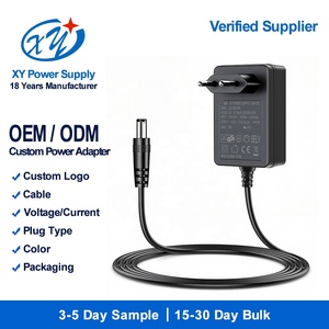
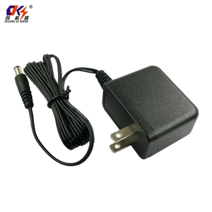
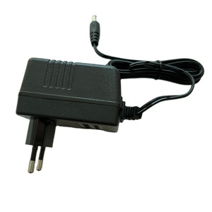
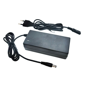
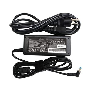
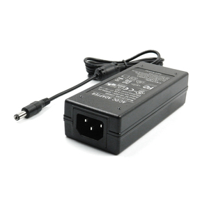
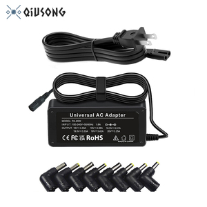
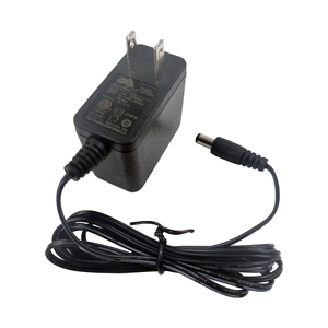
The global power electronics industry is undergoing a paradigm shift from legacy Silicon (Si) MOSFETs to third-generation Wide Bandgap (WBG) Gallium Nitride (GaN) semiconductors. As global OEMs mandate higher power densities ($W/in^3$), ultra-compact footprints, and superior thermal performance, China's power supply manufacturing ecosystem has emerged as the global epicenter for advanced GaN charger design and volume production.
Unlike conventional silicon devices constrained by a bandgap energy of 1.1 eV, GaN possesses a wide bandgap of 3.4 eV and a critical breakdown electric field tenfold higher than silicon ($3.3\,MV/cm$ vs $0.3\,MV/cm$). This intrinsic material property allows GaN High Electron Mobility Transistors (HEMTs) to operate at switching frequencies exceeding 2 MHz—compared to the typical 65 kHz – 100 kHz limitation of legacy silicon converters.
| Semiconductor Property | Silicon (Si) MOSFET | Gallium Nitride (GaN) HEMT | Engineering Advantage |
|---|---|---|---|
| Bandgap Energy (eV) | 1.1 eV | 3.4 eV (Wide Bandgap) | Higher breakdown voltage & lower thermal leakage |
| Breakdown Field (MV/cm) | 0.3 MV/cm | 3.3 MV/cm | Smaller die size for equivalent Rds(on) ratings |
| Electron Mobility ($cm^2/V\cdot s$) | 1,400 | 2,000 | Ultra-low gate charge ($Q_g$), minimal switching loss |
| Max Switching Freq (MHz) | < 0.15 MHz | Up to 2.0+ MHz | Dramatically reduces passive component size (transformers) |
| System Power Density | 5 – 12 $W/in^3$ | 25 – 45+ $W/in^3$ | Up to 60% reduction in charger volume and weight |
By dramatically elevating the switching frequency, engineers can scale down the physical magnetics (planar transformers) and output filter capacitors by up to 60%. Combined with Zero Voltage Switching (ZVS) and Active Clamp Flyback (ACF) topologies, modern GaN chargers designed by leading Chinese factories deliver peak operational efficiencies up to 95.5%, effectively halving internal thermal dissipation compared to traditional switching power supplies.
Procurement directors and engineering leads evaluating China's power supply suppliers must navigate rapidly shifting market demands driven by unified connector standards, eco-design regulations, and high-wattage mobile computing requirements:
Transitioning from standard Power Delivery (100W at 20V/5A) to Extended Power Range (EPR) delivering up to 48V/5A (240W). Demands advanced PFC + LLC resonant circuit topologies.
Multi-port (2C1A / 3C1A) architectures with embedded Microcontroller Units (MCUs) that real-time monitor output load profiles and adjust voltage/current vectors without port reset interrupt.
Strict enforcement of EU EcoDesign Directive 2019/1782, DoE Level VI energy standards, and IEC/EN 62368-1 unified safety standards across industrial and consumer sectors.
To ensure supply chain resilience, Tier-1 OEM procurement strategies now favor China factories capable of offering turnkey modified-standard solutions. Sourcing teams reduce time-to-market by utilizing pre-certified base platforms (UL, CB, CE, FCC, PSE) and customizing housing aesthetics, cable harnesses, and output voltage trims, eliminating 6 to 9 months of full compliance re-certification.
Rooted in a legacy of power conversion engineering extending over six decades, our strategic manufacturing partners in China synthesize Western power electronics engineering standards with China's unmatched component supply chain agility.
By enforcing rigorous counterfeit parts mitigation policies and ISO 9001:2015 quality management systems, our facilities ensure zero-defect shipment for critical medical, industrial automation, telecom, and consumer electronics programs.
Key technical and commercial inquiries addressed by our applications engineering team.
For standard catalog power supplies and adapters, MOQs start as low as 500 to 1,000 units. For fully customized ODM builds involving specialized plastic enclosure tooling or custom PCB layouts, initial production MOQs typically range from 2,000 to 5,000 units depending on housing specs.
GaN HEMTs feature drastically lower Rds(on) resistance and gate charge (Qg) compared to Silicon. This reduces both conduction and switching power losses by up to 50%. Reduced internal energy loss converts directly into lower heat generation, enabling passive convection cooling without noisy internal fans.
Standard catalog samples ship within 3 to 5 working days. Modified-standard samples (cable/plug changes) require 7 to 12 days. Full custom ODM projects require approximately 25 to 30 days for 3D sampling and circuit verification, followed by 35 days for mass production tooling and safety certification.
Our power supply platforms are certified to global standards including UL/cUL 62368-1 (IT equipment), IEC 60601-1 (Medical 2xMOPP), CB (IECEE scheme), CE-LVD/EMC, FCC Part 15 Class B, GS, TUV, PSE, KC, and SAA, alongside RoHS, REACH, and California Prop 65 compliance.
Yes. If your engineering specification is incomplete, our application engineers review your device load characteristics, worst-case transient spikes, physical envelope, and target operating temperatures to co-author a complete engineering specification sheet before design work commences.
We provide a standard 3-year to 5-year commercial warranty depending on the product line. Operating under ISO 9001 control protocols, our factory maintains a field defect rate target of less than 300 DPPM (Defects Per Million Units Shipped).
Speak directly with our power design engineers and OEM sourcing specialists to request product samples, custom modified quotes, or technical documentation.
Inquire Now